CCD and CMOS Sensor Info
Sensor technique - lights and darks
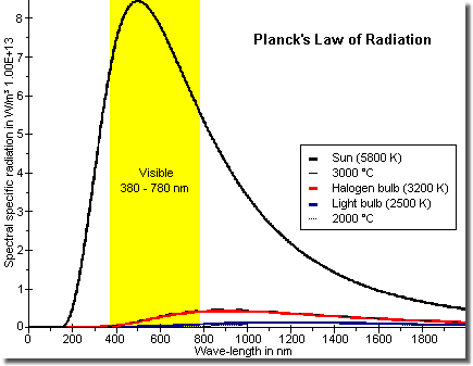
Spectral visibility of sun light and light bulbs
Evidently most of the digital cameras with semiconductor
imaging sensors, so-called solid state cameras (in contrast to bulb
or film based ones) are single-chip camera systems. This is the
reason for the lower light sensitivity of color cameras. Because
compared with the naked black-and-white (better: monochrome)
version the surface of the according color sensor is coated with a
red-green-blue (short: RGB) layer. And this swallows about 50%
intensity. Moreover the spectral sensitivity of CCD and CMOS
sensors is different to that of the human eye.
Thus often even much more is lost, because for correct color
separation and for sufficient modulation range (dynamic) the near
infrared (NIR, near IR) part of the spectrum must be suppressed by
an additional IR-cut filter (also IR-stop filter) up to about 1.1
micron wave-length. The reason is the transparency of the color
mask for light with longer wave-length and especially in this
spectral range the sensors are rather efficient. Filterless
black-and-white cameras could easily be used as cheap substitutes
for night goggles.
Perhaps in a museum or an exhibition some time ago I was lucky to
find this striking comparison of several imaging systems and their
count of different brightness scales (dynamic):
digital camera 1 K, standard slide film of the 1980s 1 M, human eye 1 Bn
Pixel and colors
Resolution - black-and-white versus color cameras
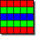
RGB stripe filter
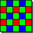
Bayer mosaic filter
Effected by the color filter coating of the sensor in stripe or mosaic pattern an additional disadvantage arises: in a black-and-white sensor each light sensitive cell contributes to the resolution directly. Each single cell can cover a tint by its gray scale value between black and white, thus each single cell represents one pixel (= picture element). A color sensor of the same quantity of cells needs one red, one green and one blue masked cell to represent a color tint. Thus each pixel consists of a RGB sub-pixel triplet of three cells. Just arithmetical the resolution in relation to the quantity of cells is reduced to one third only. These facts are held back when talking about resolution and the quantity of cells is told to be equal with the quantity of pixels. However, through complex algorithms the loss in resolution caused by the color coating can be compensated even in real time. Nevertheless, hardly more than 2/3 resolution of the according black-and-white sensor is achieved.
The images on the left show parts of color filters. Each cell
represents a (sub) pixel. The twice as much green cells are used to
enhance the resolution due to human perception capabilities (middle
of the spectrum; sensitivity). The electronics for control and
address circuits are usually placed in the black, here only thin
drawn pixel outlines. Depending on the type of sensor such a blind
area can reach and even surpass the area of the valid active
pixel then. By the way: this ratio active to passive sensor area is
named fill factor.
In general mosaic filters offer a higher resolution than stripe
filters, the color interpolation, however, is more complex.
Therefore the pixel count is not the main issue - a lot of pixel
need not to make quality (so far about the present pixel battle). At
best it is as evident as the processor clock as sole criterion of
PC efficiency. What matters is also contrast, sensitivity,
dynamics, color separation and many more. And do not forget the
lens here. A megapixel monster with slack images just inflates
memory demands with a lot of useless data in the end.
Besides more pixels per square means smaller cell sizes paired
with reduced sensitivity and increased noise tendency. (Color
pixels and even color seams appear in just black and white images
regions.)
In this context one can just check what defective pixels count
camera and sensor suppliers confront their customers with. Usually
one does not see them, because they are »mapped« by using
the interpolated values of pixels in their neighborhood. Concerning
real quality suppliers one has to search for them, whereas others
force sensors with dozens and dozens of faults upon you.
There are various color filter patterns and arrangements, not
only stripe and Bayer pattern. Usually this coating is done by
photo lithography. Also one finds other color sets than RGB, e.g.
magenta instead of red and yellow instead of blue or two different
shades of green. Also additional non-coated pixels can be
integrated in the matrix and so on.
In fact each electronic color camera gains its images by
interpolation, because there is no colored current. (Not even from
Yello. ;-). Because the color algorithm knows the corresponding
filter color above each individual grayscale cell it is able to
calculate the color at this location. As a rule several neighboring
cells are used for the calculation.
Just to mention: expensive three-chip cameras (also named 3 CCD
originally) as used in standard video applications, however, show a
uniform masked red, green and blue sensor for each color channel.
The beam split is done by a prism arrangement.
In the meantime for still cameras there are also sensors (by
Foveon) with vertical instead of lateral structure, i.e. one uses
the dependence between penetration depth and wave-length of the
light to separate the colors.
If the application is not time critical one can use color
filters or color wheels similar to those being common sight
with professional spotlights. Some studio still cameras shoot so
three successive photos each with a different color filter in front
of the sensor or lens.
Filter effects - moiré, aliasing and fix pattern noise
Effects of filters are responsible for color artifacts at
edges or lattices. If the image on the sensor is about the same
size as its filter grid or its cell structure, resp., moiré and
aliasing effects will possibly be the result. Good to visualize by
error colors in shots of Venetian blinds or fan grills. Just make a
survey with your camera. Also the effect is well-known when
scanning screened newspaper photos.
Here on principle the Nyquist-Shannon-Kotelnikov Theorem of
Sampling is valid. One can easily get an idea of subsampling
effects if one imagines to shoot e.g. a white (or gray)
fence. Then the image of each slat will have to cover at least one
row of red, green and blue pixels, otherwise the white tint cannot
be mixed. It is created only if all color channels are illuminated
with the same intensity.
Due to the fix pixel arrangement even monocolor cameras can suffer
from similar errors. Due to different partial coverage/eclipse of
pixel, beats, ghost images, occur, simply structures are shown
where none of them really is - thus »aliasing«. (This
effect often occurs when scanning newspaper or magazine photos.
Depending on resolution and magnification suddenly harsh patterns
appear due to the screened printing (i.e. grid) of the source
material.
Essentially the
Nyquist-Shannon-Kotelnikov Theorem of Sampling is valid for
(electrical) signals only. (See also
[SloMo Freq.].)
Work around for grid images: make the image unsharp; that is
nothing else then applying a low pass filter ;-)
Moiré will occurs, when two grids in the optical path are shifted
to each other, especially distorted. Then wide, large scale
streaks occur with their count and directions depending of the
angular position between both grids. This could even happen to human
eyes: just lie two finely woven fly screens over each other and
slowly change rotation angle between them.
Because each pixel provides a different dark current (i.e. does
not necessarily show »0« when not exposed), below a certain
threshold level one makes the camera electronics set all affected pixels to
black by force. Otherwise one would find scattered colored pixels
in a dark area. That limits dynamic and leads to an effect called
»drown in black« - dark surfaces and shadow areas show no
structures, inhomogeneities are wiped-out. In the beginning a major
part of digital cameras suffer from this typical deficiency.
Currently especially (cheap) CMOS cameras and notably those with
small pixel dimensions are affected.
One has even tried to use sensors with not regularly but randomly
arranged color pixels, thus without fix scheme for
positioning the single RGB color filters.
While for the color separation by penetration depth, the angular
depending path length and stochastic effects cause errors. Even
three-chip cameras can show colored lines, speckles or wedges if
beam splitting prisms are not well adjusted or separated or under
intensive illumination. Rotating color wheels can cause unstable
brightness and wrong colors when transmission differs or
synchronicity is not perfect.
Spectral sensitivity curve and spectral response
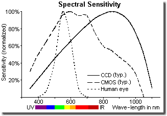
Spectral sensitivity; comparison
human eye, CCD and CMOS sensors
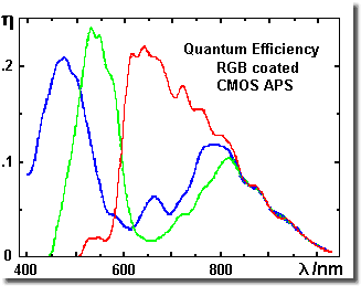
Color separation of the CMOS sensor channels;
why an IR attenuation filter is necessary
Emitted color spectrum visible for human eye (VIS) lies best case between about 380 nanometers (violet) and 780 nanometers (dark red). With the highest sensitivity in green-yellow at about 550 nanometers. CCD and CMOS sensors show a broader spectrum. Especially they work in the near infrared region beyond 780 nanometers up to the so-called bandgap of the basic material silicon at about 1 100 nanometers with a maximum sensitivity between 600 and 900 nanometers. Their maximum sensitivity is more pushed to the red compared with the human eye. (By the way: for wave-lengths beyond the bandgap silicon turns to be »transparent«.)
The figure on the upper right shows the spectral
sensitivity of the human eye in bright light mode in comparison
with that of non-coated monolithic silicon, the base material for
CCD and CMOS sensors in the visible and near infrared spectrum.
(Each curve is normalized on its maximum.)
The characteristics of CCD sensors are well given by the bare
silicon curve. CMOS sensors show a wider maximum pushed expanded to
shorter wave-length due to their flatter structures supporting the
reduced penetration depth of light with smaller wave-length.
The figure below shows the spectral sensitivity of the three RGB channels of a accordingly masked (= coated with red-green-blue filter pattern) color CMOS sensor. One clearly perceives the transparency of the polymers in the red and especially in the IR region and caused by that the demand to attenuate or respectively to block this part of the spectrum, in order to avoid overstress of red and to reduce noise, wrong level and overdriving.
CCD sensitivity: Tsutomu Sato, Spectral Emissivity of Silicon in: Japanese Journal of Applied Physics, Vol. 6, März 1967
CMOS sensitivity and RGB filter spectrum: IMEC, Leuven, Belgium
Blue filter glass: e.g. Schott BG 39 oder BG 40
When using color sensors one can manipulate this within certain
margins by selecting transmission specifications of the color
filter pattern and the arithmetical weighting of the color
channels. Additional color conversion filters (reduction of
sensitivity in red; for color video cameras often made of
bluish glass support here, too.
In the short wave-length region of the spectrum (UV, blue) the
sensors are comparatively insensitive. Besides here the glass
materials add further transmission restrictions.
The spectral sensitivity of a camera, however, is not only limited
by the sensor or the film and the filters, but also by the optics,
especially lenses and the IR-cut filters mentioned above. Because
using the full spectral sensitivity can lead to dull or blurred
images. Because the focal length is a function of wave-length, the
single color images arise in different distances to the lens
(chromatic aberration). Achromats (lens systems in layer structure)
help to avoid this effect.
Often filter (and lenses) are additionally coated in order to
reduce reflection in the visible spectrum. The reflection loss at
each air/glass interface amounts to about 4% to 5%:
ΔR = (1 - n)² / (1 + n)²
with the refraction index n of the lens material in air
(nair ☰ 1).
Thus about 8% to 10% per transmission through a glass plane.
Sometimes one happens to discover that by the iridescent colored
surfaces, when light incidents diagonally, because ΔR is a weak
function of the angle of incidence.
Lenses of higher quality sometimes offer an IR switch for
operating exclusively with wave-lengths in the near infrared of
about 780 nanometers and more. Then the inscription on the distance
ring will fit again. (The IR image is displayed deeper inside the
camera, due to smaller refraction of longer wave-lengths.)
By the way: the transmission of standard lens glass heavily
decreases with wave-lengths of 320 nanometers and less. In the long
wave section the drop lies far away from what a sensor made of
silicon perceives. Just to mention the coating layer of a sensor is
made of quartz glass (silicon di-oxide). It is covered by a thin
layer of silicon nitride.
If one wants to make shots in an other region of the spectrum, one
has to use different sensor and even lens materials. For instance
IR cameras and especially thermography cameras, which work in the
wave length region of about 3 micrometers and above, partly use sensors
made of Indium-Gallium-Arsenide (InGaAs).
CCD versus CMOS sensors
Function principles
Each of both present solid state sensor technologies CCD (charge coupled device) and CMOS (complementary metal oxide semiconductor) are designed with silicon as raw material. Their advantages and disadvantages depend on their basic functions. They use the inner photoelectric effect - in both the pixel work like an array of solar cell panels on the rooftop or in a meadow: one pixel = one solar cell, more light = more charge or current, resp.
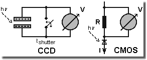
CCD and CMOS circuit principles
The image on the left shows the basic principles of
a CCD cell in comparison with a CMOS cell.
The charge generated in a CCD cell by incident light is directly
read out from each cell. This charges are moved step by step
outside of the photoactive area, so CCD called bucket chain
principle. Outside they are analog-digital converted and amplified,
resp.
In the CMOS cell the incident light generates a photo current
proportional to its intensity in each cell and decreases the
reverse resistance of each photo diode. These reverse currents
through the photo diodes (i.e. the generated charges) are
processed.
The cells of a CCD sensor operate as exposition meters
accumulating charge and are read out in certain intervals. The
fast CCD sensors exist in three types: FT ((Full) Frame Transfer),
ILT (Interline Transfer) and FIT (Frame Interline Transfer). For
still photography the full frame principle is sufficient enough:
The charges remain in the active area until read-out shaded by a
central mechanical shutter.
In FTs the complete frame is moved through the photo active cells
in a separate light shielded area and then it is processed. Due to
the different structures often it is possible to identify both
regions by one's naked eyes. ILTs show alternating photosensitive
and read-out lines. The charge of each photoelectric cell is
directly pushed to the according light shielded neighboring cell
and this line is then read-out. FITs are a combination of both
designs.
FTs reach a fill factor of almost 100%, but suffer of a second
exposure during the read-out phase (so-called smear). ILTs and FITs
show a reduced fill factor, but are less sensitive in read-out
phase.
The expression fill factor gives the ratio between optical
sensitive area and area occupied by addressing circuits of each
cell. Thus it allows to compare sensitivity under the precondition,
however, using the same basic technology.
CMOS sensors continuously measure the light induced photo
current. One uses the proportional relation between reverse current
or induced charges, resp., and exposure of a photo diode.
(Expressed in correct terms one measures the current to re-charge
the reverse capacity at the pn junction inside the photo diode. One
can imagine a capacity parallel-connected to the diode being
discharged by incidence of light. There are different possibilities
for appropriate circuits.)
The cell structure and wiring are rather similar to the layout of
a DRAM, and so experimental shots were already made with ground
(i.e. removed molded plastic housing) memory circuits.
A PPS (Passive Pixel Sensor) operates like a CCD ILT. By
illumination caused charges generated in a photo sensitive cell,
mainly a photo diode, are read out cell by cell directly and are
amplified and analog-digital converted outside the photoactive
area.
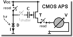
CMOS APS cell with global shutter
Common nowadays is the APS principle.(Active Pixel Sensor. The
acronym has nothing to do with the APS-C format.) Here photo
sensitive cells just work with the indirect principle of a CCD
sensor: the exposure of a photo diode controls the connection to
the operating voltage Vcc using a CMOS transistor (amplifier). Each
cell just has its integrated amplifier circuit.
Because illumination reduces the charge over the photocell one can
compare it with the negative film inside a camera.
The figure on the left shows the structure of a CMOS APS cell. Description of one cycle: over the reset switch a pre-charge is brought in. After that the switch opens again and over the photo diode D related to illumination charge floats off. With that the control voltage at the amplifier T changes and with it the voltage V. Using the optional switch t shutter (if available) one can interrupt the discharge process, then the capacitor C controls the amplifier T all alone.
The pre-charge (realized by the reset switch), each time during
exposure reduced by the photo diode, is the reason for CMOS APS
being insensitive to saturation effects unlike CCD sensors. More
than complete discharge is not possible.
The simplest cell is made of three transistors, namely the switch
for the initiation before starting the frame/exposure (reset), the
switch for read-out process (read) and the real amplifier (T). This
circuit offers a rolling shutter only. If one adds some kind of
sample and hold circuit (t shutter and capacitor C) in the
amplifier control circuit one will get a global shutter. This is an
electronic shutter operating on the whole sensor at one given
time and not only line by line like the rolling shutter, which is
similar to a falling curtain.
With more transistors one receives additional opportunities for
controlling and improving the signal quality. Thus using a five or six
transistor cell one can decouple recording and read-out, so already
start recording or exposure, resp. again during the read-out
process is still running.
CCD sensors
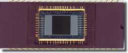
EG&G Reticon Frame-Transfer CCD sensor
HS0512JAQ; 512x512 pixel in 8.19x8.19 mm²;
ceramic DIP housing; >1 000 fps, monochrome
-
are in production and in use for some decades
-
provide good images by nature, otherwise one would sort out the doubtful sensor and will not use it at all
-
can (as FT) reach a fill factor of almost 100%
-
are also sensible in near infrared (therefore especially many color cameras are equipped with an IR-cut filter)
-
often need more than one supply voltage and show a high power consumption
-
are several times more sensitive to light - in positive as in negative manner. One could shoot with less illumination, but the sensors are sensitive to overexposure. Thus very bright regions show flare-shaped extinction (blooming) in the neighborhood, which can cover the complete frame; high irradiation during read-out phase can lead to some kind of double exposure (smear).
-
are only well done by specialized semiconductor manufacturers. With increasing count of pixels there is a dramatic yield decrease, because due to the basic function, especially in FT sensors, the optical active regions are used as wire during the read out phase. A defect cell can paralyze a complete line or column. Then the sensor is not to use.
CMOS sensors
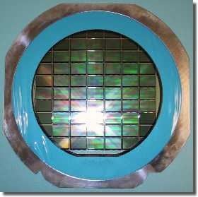
6 inch wafer; 45 CMOS sensors on blue tape
-
are more noisy because of their not homogeneous structure and show similar problems as flat panel displays. Some error pixels may occur, which will be computed away then. One has to put emphasis on the image processing (among others masking defective pixels so-called mapping). Each pixel is adjusted individually (gain/offset settings).
-
may reach a fill factor of about 50% and therefore in general they need usually more illumination
-
are as APS (active pixel sensor) almost completely insensitive to overexposure. PPS (passive pixel sensor), however, are a bit more critical
-
show about the same spectral sensitivity (i.e. color perception) as the human eye
-
often need just one supply voltage and show a moderate power consumption
-
come from the much more present technology. Assuming a sufficient quantity they are significant cheaper. Besides read out is made with additional lines, thus a defective pixel can be interpolated by its neighbor pixels and does not ruin the sensor.
-
offer the possibility to integrate additional circuits or signal pre-processing on the same chip in order to shrink the camera and to increase flexibility; the more or less random access to the single cells makes possible e.g. the pre-selection of a window, so called sub sampling, windowing, ROI (region of interest) or AOI (area of interest). Also image processing for trigger events (in frame trigger) or a second exposure run in each frame are comparatively easy to realize.
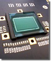
Bare CMOS sensor die for COB mounting
1536x1024 pixel on 16.9x11.3 mm²; >1 000 fps,
color
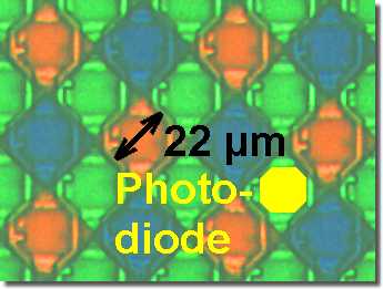
Color filter in diagonal arrangement (magn. 1 000 x)
State of the art
Evidently still many of the photo and surveillance
cameras use CCD sensors, while it is not possible to imagine
up-to date photo and video cameras without CMOS sensors. In mobile
phones with camera function CMOS sensors are used almost
exclusively. The trend moves to CMOS technology, to the
camera-on-a-chip.
In high-end cameras temporarily one has sometimes tended towards
low integration yet to optimize each part like analog, digital
electronics, control, power supply ... individually. In standard
use none of both techniques just supersedes the other one. In noise
critical special applications, however, the CCD sensors lie in
front. Cooled if necessary. For shots against illumination sources
and possible overexposure effects (shiny surfaces ...) CMOS
sensors may be the better choice.
By the way: the often made assertion CCD sensors are in principle
slower than CMOS sensors is not true so far, because there are CCD
high-speed camera sensors available as well, see e.g. the sensors
of Dalsa or EG& Reticon.
Images on the upper left: silicon die without housing, about
20 mm x 15 mm x 0.5 mm in 0.5 micron technology. The
greenish area is the mosaic filter. In the framing dark border one
recognizes 137 small squares, so-called bond lands or pads, for the
later electrical contacting with bond wires.
This die is directly, thus without housing, glued on the printed
circuit board and is bonded then chip on board (COB). After that
for protection reasons a cover with glass bottom is put over and is
glued to the board. (Of course, traditionally housed sensors are
available as well.)
Image on the lower left: 1 000 times detail magnification out of the filter matrix of the CMOS sensor. The light sensitive area of the photo cell, marked yellow in the image, shows with 11 microns half of the cell size of 22 microns. The chessboard pattern tilt by 45° built with honeycomb cells like Fuji and Sony successfully use it in their »Super-CCD« and »ClearVid« arrangement resp. allows a higher resolution especially of vertical and horizontal structures compared with the standard Bayer pattern.
Also according high-speed cameras this change was obvious.
Whereas typical systems of the 1990s still used modified CCD sensors
in general, systems since the end of the 1990s mostly operate with
CMOS sensors. Nevertheless, CCD sensor systems exist further
on.
Well known high-speed camera sensor sources are Dalsa/Teledyne
(Canada), EG&G Reticon (USA), Fillfactory/Cypress (Belgium),
Photobit/Micron/Aptina (USA) or CSEM (Switzerland).
Lenses and optics
Lens mount, flange-back (back focus), focal length and crop factor
Elementary criterion for selecting lenses is to check which mount is given by the camera body. The mount determines the flange-back or back focus distance. It is the distance measured between the last cylindrical landing of the lens housing before the thread and the film or sensor plane. Thus the distance between optics and image plane is mount specific. With a lens out of a different mount family possibly the focal length inscription of the lens is not correct, as far as one can adjust its focus and fix it at all. The flange-back e.g. with C-mount is 17.562 mm and with CS-mount it is 12.5 mm. When one happens to get a more or less sharp image of the iris aperture and nothing else, one has screwed a CS-mount lens on a C-mount camera. (But with a 5 mm spacer a C-mount lens fits onto a CS-mount camera.)
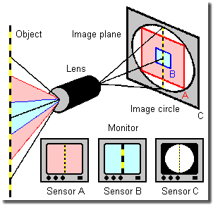
Image circle, format and crop factor
Within a mount family there are not such problems. All adequate lenses show the same flange-back, thus each image is displayed at the same location. The only difference is the varied size of the circular images the lenses offer at the image plane. Given is the format of the sensor that is illuminated sufficient enough and without too strong optical distortions. If the sensor completely lies inside this image circle, everything will be all right. If it is larger, the shot images will be considerable sharp, but their corners tend to be underexposed (keyhole effect, vignetting). Thus especially one can usually select without problems C-mount lenses of larger formats for a C-mount camera with a smaller one, e.g. an 1 inch lens on a 2/3 inch camera. In the other way, however, with restrictions only, see sensor C in the figure on the left.
The figure on the right shows the crop factor, also
named focal length extension. This is in fact a pseudo effect,
because focal length is an invariable attribute of each lens. How
could the lens ever know which sensor is operated? The different
image impression, especially the angle of view (also field of
view), is only caused by showing the image of a smaller sensor (B)
with a greater magnification on a screen or a print. Its pixels lie
closer to each other than those of a bigger one (A) and are
displayed somehow stretched, nevertheless, without negative effects
on quality. Adequate resolution (pixel count) assumed.
At least the sensor must lie inside the image circle of the lens,
given as format, otherwise vignetting takes place (C).
If one compares two format filling images of an object, e.g. one
of a C-mount camera with a 2/3 inch sensor and one with an 1 inch
sensor, usually one will not see a difference. Displayed on the
monitor screen they are of the same size.
But due to the fact that they come from areas of different sensor
sizes, the magnification must be smaller on the smaller sensor
(here B), in order to make the image fit to it. Therefore the same
»XY Millimeter« lens in front of a larger sensor (here A)
will work at a camera with smaller sensor like one with a larger
focal length and vice versa. But this will be exclusively valid
only if one compares the shots based on the angles of view (= what
fits onto the respective sensor using the same lens). So far focal
length and image format belong together and give the imaging scale.
The image circle, however, is a lens parameter only. And the focal
length, too. (Thus the sensor size alone is responsible. It is a
pity, but it is not written on the camera housing.)
Perhaps one could introduce the term »effective focal
length« in respect to field of view change, but related to
what? Well, often in common usage this dummy effect of focal length
extension is called (digital) crop factor:
crop factor = 43.3 mm / sensor diagonal [mm]
The value (about 1.5 to 2 comparing typical digital SLR cameras
with35 mm miniature format cameras of 24 mm x
36 mm and thus 43.3 mm diagonal; therefore sometimes the
expression »XY mm 35 mm format equivalent«) states the
apparent increase of the focal length finally due to the decreased
sensor diagonal. Thus the expression »crop« meets the facts better.
Much of the image just misses the smaller sensor. One will see the
center only and will interpret this as tele/zoom effect, when the
monitor is displaying the sensor full screen, see the figure
above.
Hooked on high quality demands one has to take into consideration,
however, that the area with optimal corrected lens errors is
smaller than the maximum illuminated one and that smaller formats
claim lenses of better qualities because of the higher pixel
density. Besides one should not spoil the image quality of a good
camera by using just a better bottom of a bottle instead of a lens.
Then the image remains sharp to the corners.
In professional still imaging widespread use of the according
possibilities is made.
If the focal length of a lens is of about the same value as the
diameter of the format, one will often call it the »normal lens«
for this format. Concerning miniature or 35 mm cameras this
would be about 50 mm ±5 mm, see next chapter
and [SloMo Tips].
Then the (sharp) angle of view equals that of humans
roundabout.
Formats
Elementary feature, too: usually the format or film gate, i.e. the size of the optical active area on the CCD or CMOS sensor, is given for CCTV cameras in inches. The somehow arbitrary dimensions are from the Vidicon valve era. The data derive from the size of their (socket!) dimensions. As base for the inch class of a sensor the 1 inch sensor with a diagonal of about 16 mm is used:
Inch format ≈ sensor diagonal [mm] /
16 mm
or when using inch measurement:
inch format ≈ sensor diagonal [inch] / 1.5875
although in real one inch measures 25.4 mm. A smaller sensor makes the camera smaller and, of course, the nominal sensor yield per wafer during fabrication increases.
| Format [inch] | Width [mm] | Height [mm] | Diagonal [mm] | Remark |
|---|---|---|---|---|
| 1/10 | ~ 1.44 | ~ 1.08 | ~ 1.8 | autonomous CCD camera for medical in corpore use (to swallow like a pill) |
| 1/8 | ~ 1.626 | ~ 1.219 | ~ 2.032 | CMOS cameras for special applications |
| 1/7 | ~ 2.055 | ~ 1.624 | ~ 2.619 | CMOS cameras for pads, smart and mobile phones ... |
| [128² pixels] | 2.048 | 2.048 | 2.896 | Dalsa CA-D1-0128A CCD, 736 fps (tweaked 2 020 fps) |
| 1/6 | 2.4 | 1.8 | 3.0 | single board cameras for special applications |
| 1/5 | 2.88 | 2.16 | 3.6 | single board or simple cameras, webcams ... |
| 1/4 | 3.6 | 2.7 | 4.5 | cameras for observance (typical with pinhole lens) |
| [256² pixels] | 4.096 | 4.096 | 5.793 | Dalsa CA-D1-0256A CCD, 203 fps (tweaked 531 fps) |
| 1/3 | 4.8 | 3.6 | 6.0 | cameras for automation (»machine vision«) |
| 1/2 | 6.4 | 4.8 | 8.0 | above all portable TV video cameras, often 3 chip version |
| 1/1.8 | 7.2 | 5.4 | 9.0 | standard still (CCD/CMOS) cameras |
| 2/3 | 8.8 | 6.6 | 10.991 | standard in the image processing sector |
| [512² pixels] | 8.19 | 8.19 | 11.582 | EG&G Reticon HS0512JAQ CCD, 1 000 fps (tweaked 1 094 fps) |
| 16 mm film (movie) | 10.3 | 7.5 | 12.7 | 16 mm film cameras (Stalex, HYCAM), 3 000 fps, 10 000 fps |
| 1 | 12.7 | 9.525 | 15.875 | professional (studio) TV video cameras |
| [1280x1024 pixels] | 15.36 | 12.29 | 19.67 | Photobit MV-13 CMOS (Aptina MT9M413C36ST C/M), 500 fps |
| [1536x1024 pixels] | 16.896 | 11.264 | 20.306 | Weinberger FhG/CSEM Cam 2000 Visario CMOS, 1 106 fps |
| 1¼ (30 mm) | 17.1 | 12.8 | 21.4 | professional (studio) TV video cameras |
| 4/3 (»Four Thirds«) | ~ 18.0 (not def.) | ~ 13.5 (not def.) | 22.5 | semi professional digital SLR (photo) cameras |
| 35 mm film (movie) | 22.05 | 16.03 | 27.28 | professional 35 mm film (movie) cameras |
| APS-C | (24.0) 25.1 to 25.5 | (16.0) 16.7 to 17.0 | ~ 30.15 | APS-C film and sensor cameras |
| miniature or 35 mm | 36.0 | 24.0 | 43.3 | 35 mm (photo film) cameras and »full format« digital cameras |
Sensor sizes and formats. Legend: fps = frames per second. (In
green some selected high-speed camera matrix sensors.)
Aperture (f-stop)
Exposure - the aperture or f-stop adjusts the
incident light intensity falling on the sensor or film. The f-stop
number is defined as k = focal length / effective opening diameter.
On the f-stop adjustment ring one finds the f-stops inscription as
multiples of the square root of 2 (1.4 - 2 - 2.8 - 4 - 5.6 - 8 - 11
- 16 - 22 - 32 - ...). With increasing f-stops the intensity let
through is reduced in a way that one receives half of the intensity
from step to step.
The reciprocal of the smallest f-stop number is often called
»transmission« or »light strength«. But if one
wants two lenses offering the same brightness, one will have to
take two with identical t-stops, defined as t = 10 x f-stop /
√ transmission [in %], as it is usually provided by lenses
for movie cameras.
When using a sensor with the same size a smaller aperture diameter
(= high f-stop number) enlarges the depth of view, see
[SloMo Tips].
Zoom lenses, digital lenses and resolution
Expression zoom stands for lenses, which permit to tear
closer an object by using a stepless focal length increase within a
certain range of given focal length. Usually they are large, heavy,
expensive and of poor light sensitivity. One should prefer to use
exchangeable lenses of different but fixed focal length. There are
available real zoom lenses, where the image stays sharp during
zooming, and vario focus lenses, where one can change the focal
length, too, but has to adjust focus as well.
»Digital zoom« or »electronic zoom« stands for
an enlargement of a part of an image by means of a (simple) imaging
program. High zoom levels cause pixeled images. Normally electronic
zoom is not a worthy substitute of an appropriate zoom lens, even
if marketing likes to claim it so.
By the way, similar case: »5x zoom« does not say
anything about the magnification of a lens, but merely that its
smallest adjustable focal length is five times smaller than its
biggest.
Especially in the meantime
»digital« lenses or sometimes also called telecentric
lenses are offered. They are designed so that the beams at the
image side hit the sensor in an angle as perpendicular as possible.
This is done to accommodate the shaft-like structure, which
especially has a bad influence on small sensors with high pixel
density, causing faults like diffraction, shadows, color errors,
flattening ... (Just the small, cheap sensors need complex and
expensive lenses.)
To call such lenses telecentric, however, is infelicitous. Namely
this type of special lenses images an object in the same size
disregarding its distance. These optics are especially used in
image processing for measurement applications. For instance if one
views in a tube, it will not become narrower with increasing
distance, but it will look like a ring washer and it will be no
problem to measure the inner diameter and the thickness of the
wall. Used with an usual landscape scenery strange effect may
occur, e.g. roads running to the horizon do not get smaller.
When talking about resolution it is highly recommended to get an idea of the modulation transfer function MTF, find an excellent explanation e.g. in quality features of lenses as part of the knowledge hub of Schneider-Kreuznach.
Image plane offset
Exotic in most cases - with not perpendicular incidence through a plane-parallel plate a lateral offset occurs. When one screws a thin filter in front of the lens, this will rarely have any effects on the imaging position of the optical system due to the in most cases large object distance. But this will drastically change if one adds a protection glass, a filter or a LC shutter behind the lens. These plane-parallel plates cause some kind of glass delay effect (additionally)
Δd = (1 - 1/n) × d
with the refraction index n and the thickness d of the
plate (nair = 1).
With a glass plate the image would appear about 1/3 of its
thickness behind the sensor, due to the increase of the effective
flange-back. A mechanical solution must be designed in order to
adjust this certain additional distance between lens and camera
body, exact the sensor.
Therefore the threaded pins or special mechanics, resp. in the
lens adapters e.g. for cameras prepared for optionally mounting an
internal LC shutter or an additional internal (IR-cut) filter, or
which are designed for IR shots.
Sensor improvements
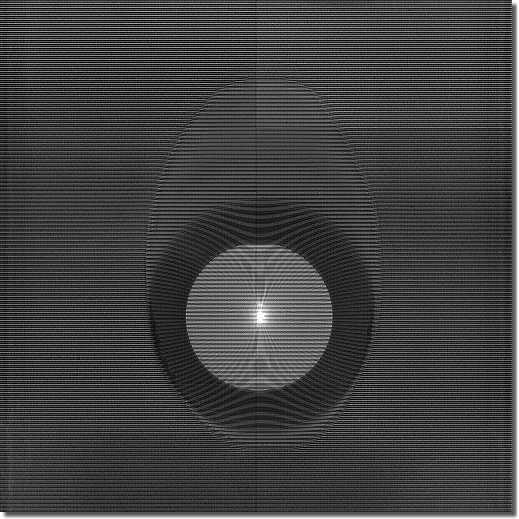
Drop of glue on optical sensor chip - refraction effects
The photo on the left shows an extended glue drop on the surface of EG&G Reticon Frame Transfer CCD sensor HS0512JAQ as mentioned above during [Photo Color] filter adjustment. It was shot using the sensor itself.
Microlenses
Everything counts in large amounts. Because of a fill
factor, i.e. the ratio photoactive area to control electronics
area, smaller than one area and therefore sensitivity is
lost.
The structure of CMOS sensors makes it worth to try micro lenses
in order to compensate this lost at least partly. The lenses should
transport the light falling on the blind sticks to the light
sensitive parts of each cell. Especially one likes to use them for
very small cell structures and fill factors (ten micrometers per
square cell size and 30% fill factor and less). The lenses are
directly deposited on the sensor surface by photo lithography. Due to
the small size of the lenses, diameter a few hundredths millimeters
each, and the large quantity - one lens for each cell (= pixel) -
it is a certain endeavor and the optical qualities and the
uniformity are not quite improved. This causes an
under-proportional increase of sensitivity. The price is higher
expense and possibly reduced image quality due to optical faults
and other parasitic effects.
BSI (back side illuminated) and stacked sensors
Eyes and especially CMOS sensors show a quite similar
layer structure. In both the light must pass a shading supply layer
- blood vessels or electric circuits, resp. - before received in
the photoactive layer. Fill factor and image quality are reduced.
Moreover with further shrunken structures in semiconductor design a
trade-off between what is good for electronics and what is
necessary for optics occurs. Shrinking and higher clock rates and
reduction of power consumption as well cause noisy small
photocells. For instance standard design rules (structure size,
width of conductor paths, gate width) of present DRAM and CPU
techniques do not match CMOS sensor demands by a factor 50 or more.
(At present serial structure width is about 10 nm only.)
Besides the transistors in logic circuits are trimmed for speed and
digitally switch (bang-bang, on/off), while
photoelectric elements should be read out analog and a saturation
should be preferably avoided.)
Therefore the idea to grind the sensor bottom and then to put the
sensor die upside down. The supply electronics are at the bottom,
the middle is filled by photocells and on the upper side color
filter pattern and perhaps micro lenses are placed. The sensitive
layer is illuminated from the rear side, therefore its name.
The gap between CMOS standard designs and sensor demands can be
red uced by that, what makes the sensors cheaper especially by
integrating further electronics and conceals deficiencies like e.g.
the meanwhile not deep enough p/n junction layer position for the
penetration depth of light beams.
Not really a quite simple semiconductor process (among other
massive grinding of the wafer is necessary), but similar technique
was used with special CCD sensors, too.
Some rare photo cameras make use of stacked chips or layers, the
sensor IC lies on top of the control and/ore memory IC or layer,
resp.
Often, however, the sensors are produced in technology families
with bigger structure widths than that of present DRAMs or
processors. This is especially valid concerning high quality
cameras.
Scientific CMOS (sCMOS)
Enhancement by combining the best of both worlds,
bridging the gap between CMOS and CCD. Contrary to cameras for the
mass market the pixel count for cameras used with technical and
scientific applications is not the sole criteria. One rather tries
to define for these areas of applications (e.g. microscopy) an
optimal combination of resolution, dynamic, speed ... Especially
one aspires to improve sensitivity and noise suppression of the
CMOS circuit design with photo cells as large as possible and with
extra designed-in sophisticated analog-digital converters on
pixel and line or column level. That requires area, of course, so
at least early sensor designs just provided a rolling shutter. The
global shutter so essential for high-speed videos could just be
missing sometimes.
Meanwhile even fast BSI sCMOS sensors are available.
Extend the [TOUR] to Tips and tricks about making sequences.

